Meet us in person or follow os online.
These are also to be integrated directly into the production processes as far as possible to ensure both high-precision characterizations of the components as well as control and optimization of production. The precision metrology from Task Group F1 will be combined with the concepts developed in Task Group F2. To create an automated, self-optimizing production chain, F2 uses concepts for adaptive control of production and the realization of a virtual component model ("digital twin") based on artificial intelligence (AI) approaches.
The comprehensive measurement data generated in Task Group F1 also serves as input for the multiscale simulations developed in PhoenixD. These simulations of both the component functionality and the manufacturing processes provide a deeper understanding of the underlying physical effects and dependencies during manufacturing and resulting in novel optical systems for applications.
Examples of such applications include biomolecule detection, point-of-care diagnostics, environmental monitoring and medical imaging and analytics.
How does this aspect fit into PhoenixD's overall strategy of developing and building novel optical technologies?
Task Group F1 develops both new, real-time capable inline measurement techniques for integration into the manufacturing processes and high-precision offline metrology for the precise characterisation of the manufactured optical components and systems.
On the one hand, these are necessary for the realisation of adaptive manufacturing chains and, on the other hand, should provide important insights into the functionality of the optical systems, material and process development as well as multi-scale simulation.
Ultimately, this will enable (i) an integrated and resource- and cost-efficient production of precision optical components and systems in a fully interconnected and automated production environment, especially also for small batch sizes, (ii) a comprehensive multi-physical description of all relevant effects and (iii) validation of the functional systems for new applications.


 ©
Tim Wolfer, Christian Kelb
With which other working groups do you work particularly closely for this?
The activities of Task Group F1 correlate closely with, for example, the development of the concepts for adaptive production and realisation of the virtual component models (Task Group F2), material development, additive manufacturing and integration (Task Groups M1, M2, M3 and M6) as well as the simulation of optical materials (Task Group S2) and linear and non-linear system functionalities (Task Group S3).
The most comprehensive multi-physical description of optical functions and processes possible requires verification of the simulations by experimental data to develop efficient yet physically correct models for the materials used and individual optics researched (Task Group S2 and S3).
PhoenixD aims at interconnected processes in production to realise continuously complex optical systems in a process chain. Close coordination with all batch and continuous production technologies is required here (e.g. with Task Groups M2 and M3).
For the functionalisation of the optical components, the connection to researchers in data sciences and information technology is essential. They develop suitable optoelectronic interfaces, which help create the individual virtual models for each system and implement the AI algorithms to improve future production based on real-time measurement data.
What applications could you envision in the future based on the current state of affairs?
The main applications are in the multiplex detection of biomolecules in the life sciences and medicine, the monitoring of toxins in the environment, the monitoring of food production and production processes in the industry, medical point-of-care diagnostics and the optical monitoring and control of plant growth in digital farming. Individualised, adaptive, and learning systems realised using additive manufacturing methods can open up new applications or cover existing needs in science, business and industry.
Our Motivation
Functional optical systems can offer useful alternatives to electronic-based solutions. However, their production is currently still quite complex and therefore in many cases, neither cost-efficient nor resource-efficient.
The development of modern, additive manufacturing methods combined with artificial intelligence algorithms for processing large amounts of data, can lead to a revolution in optics manufacturing in the future. Global trends such as Industry 4.0 or the Internet of Things have already indicated these technologies' great potential. The prerequisite for this revolution in optics manufacturing is that such manufacturing methods can produce individual elements and even entire functional systems with an integrated optical quality.
Our activities focus on research into the production of micro-optical and nano-optical components based on polymers and their application for sensory and metrological tasks. To achieve this goal, we develop high-precision and real-time measurement technology, which is necessary to detect inaccuracies in production already during the process and correct them in connection with an equally real-time functional simulation.
In particular, we also use new types of materials in the production of optical elements, which on the one hand allow new system functions and on the other hand take the sustainability aspect into account during production. Ultimately, this should minimise the consumption of resources and the ecological footprint of the new components and systems and reduce the costs to such an extent that they will be available in the future to broad fields of application, some of which are currently not possible, in all walks of life.
Our Research
We use additive and subtractive manufacturing methods to realise sensory-optical functionality. The methods applied include, for example, direct writing by laser, photolithography, or imprint replication. As material classes, we use photosensitive polymers.
The systems required for a metrological task are realised through micro-optical and nano-optical elements and assembled into complete functional units through 2D and 3D integration. In addition to precise manufacturing based on an optimised design model, real-time monitoring and adaptation of production and comprehensive characterisation of the components are crucial for their functionality.
The development of a self-optimising manufacturing chain requires its implementation in a closed-loop (feedback loop), which continuously feeds back using precision metrology. In this way, errors in production can be detected and compensated for during simulation and manufacturing.
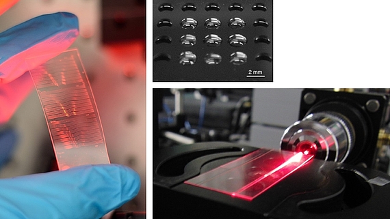
Precise offline measurement technology shows the functionality of the manufactured components. For the analysis, we apply technologies, such as interferometry, as well as optical and atomic force microscopy, gaining insights into the behaviour of the materials structures and the measurement function.


 ©
Lei Zheng/HOT
Inline metrology, e.g. based on near-field measurement concepts or spectroscopic ellipsometry, is integrated into the process chains to check the quality of manufactured structures and correct them if necessary. Coherent X-ray metrology is also used in the long term to enable measurements independent of material parameters.


 ©
Axel Günther/HOT
To realise this vision, cooperation with many working groups of the Cluster of Excellence PhoenixD is necessary. For example, the Cluster's scientists develop new materials, with which passive and active elements can be created. The development of manufacturing methods for hybrid materials and their modelling and simulation is also relevant to our research.


 ©
Emil Agocs/HOT
Besides, we work closely with the Task Groups that deal with 2D and 3D integration, functional coating and electronic control of the systems (Task Groups M5 and M6).
Finally, the machine and characterisation data collected in the process is fed back into the manufacturing process by suitable interfaces. The information supports creating a constantly self-optimising production environment with a closed feedback loop (Task Group F2). For this purpose, we cooperate with Task Group S4, which develops suitable interfaces and handover points.
Contact


30167 Hannover


